

As the battle to win in the semiconductor industry intensifies, particularly in the burgeoning field of AI chips, industry players are realizing that a key technology called electronic design automation is essential to gaining chip advantage.
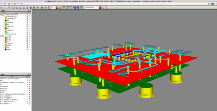
EDA tools design, verify and simulate the chip manufacturing process to ensure the required performance and density are achieved.
Even after a chip is manufactured, such tools are essential to ensure that the device that contains the chip continues to work as expected throughout its lifetime.
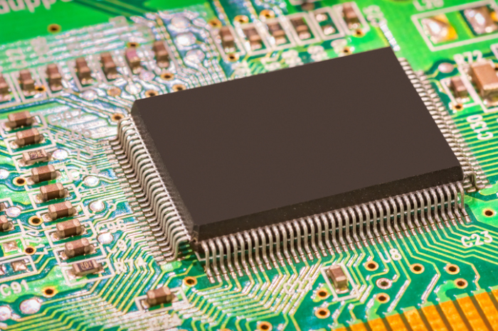
Given that cutting-edge devices contain more than a billion circuit elements, industry insiders say it would be impossible to design and manufacture today’s semiconductor devices without EDA tools.
If an error occurs in a manufactured chip, they said, the costs could be catastrophic because the error cannot be “fixed” — the entire chip would have to be redesigned and remanufactured.
“With the rise of high-bandwidth memory and AI chips, error-free chip stacking is more important than ever,” said Lee Jun-hwan, CEO of Seoul-based EDA tool provider Baum Design Systems.
The company has been working on developing new EDA tools since it was founded in 2013 but has struggled to hire EDA engineers in South Korea, he said.
“We are struggling to recruit talent. Talented engineers are leaving the country simply because the EDA ecosystem does not exist here,” the CEO said.
Top in HBM but unknown in EDA
South Korea is home to the world’s two largest memory chip makers, Samsung Electronics and SK Hynix.
In recent years, the two memory giants and their overseas rivals have been building up capacity to make high-bandwidth memory (HBM) chips in an effort to capitalize on the AI boom.
HBM offers much faster processing speeds than traditional memory chips, making it a vital part of the AI boom.
SK Hynix is a major supplier of HBM chips to Nvidia Corp., the world’s top AI chip designer. Samsung is also looking to supply HBM products to Nvidia.
“South Korea leads the global HBM market, but I have to say that the EDA technology that can integrate AI and HBM does not exist in South Korea,” said a South Korean chip industry source.
With the governments of China and Taiwan actively supporting their domestic EDA companies, South Korea is also beginning to take action.
Following instructions from Minister Lee Jong-ho, the Ministry of Science and ICT recently began contacting domestic EDA companies and investigating the situation.
“Just three years ago, government officials didn’t even know the concept of EDA. Fortunately, they now understand its importance,” said an executive at a South Korean EDA company.
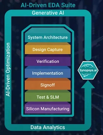
Synopsys, Cadence, Siemens EDA
The global EDA tools market is dominated by US companies.
According to market research firm TrendForce, the leading EDA technology provider is Synopsys with 32% of the market, followed by Cadence Design Systems with 30% and Siemens Digital Industries Software (also known as Siemens EDA) with 13% market share.
Samsung, SK Hynix and major fabless chip design companies use EDA software developed by these three companies.
There are only a handful of EDA companies in Korea, including Baum and Alsemy.
According to industry insiders, there are about 300 EDA companies in China, of which the top 10 are known to be delivering advanced technology despite U.S. sanctions.
According to British market research firm EMIS, the global EDA market is expected to grow from $10.8 billion in 2020 to $18.37 billion by 2026.
China sees opportunity in South Korea
The Shanghai government recently announced measures to support the EDA industry, including a 30 percent subsidy for new investments by EDA companies.

Industry sources said Huawei was likely working with Empyrean Technology Co., China’s largest EDA company, to develop the 7-nanometer chips.
“Recently, Chinese EDA companies have been entering the Korean market by setting service prices at half those of U.S. companies. They have very strong price competitiveness,” said a source in the Korean semiconductor industry.
China’s three largest EDA companies, Empyrean, Primarius Technologies Co. and Entasys Design Inc., have been Samsung Foundry’s partners since 2022.
“It’s time for the South Korean government to pay more attention to the EDA sector from the perspective of economic security,” said Kim Young-seok, a professor of semiconductor fusion engineering at Sungkyunkwan University.
Write Kang Kyung-ju qurasoha@hankyung.com
This article was edited by In-Soo Nam.